Purpose
The RT6212A is a synchronous step-down converter with the input voltage range from 4.5V to 18V and provides 2A output current. This document explains the function and use of the RT6212A evaluation board (EVB), and provides information to enable operation, modification of the evaluation board and circuit to suit individual requirements.
Introduction
General Product Information
The RT6212A is a high-efficiency, monolithic synchronous step-down DC/DC converter that can deliver up to 2A output current from a 4.5V to 18V input supply. The RT6212A adopts ACOT architecture to allow the transient response to be improved and keep in constant frequency. Cycle-by-cycle current limit provides protection against shorted outputs and soft-start eliminates input current surge during start-up. Fault conditions also include output under voltage protection, output over current protection, and thermal shutdown.
Product Feature
-
Integrated 163mΩ/86mΩ MOSFETs
-
4.5V to 18V Supply Voltage Range
-
500kHz Switching Frequency
-
ACOT Control
-
0.8V±1.5% Voltage Reference
-
Internal Start-Up into Pre-biased Outputs
-
Compact Package : TSOT-23-6 Pin
-
Over-Current Protection and Hiccup
Key Performance Summary Table
|
Key Features
|
Evaluation Board Number : PCB039_V1
|
|
Default Input Voltage
|
12V
|
|
Max Output Current
|
2A
|
|
Default Output Voltage
|
1.2V
|
|
Default Marking & Package Type
|
RT6212AHGJ6F, TSOT-23-6 (FC)
|
|
Operation Frequency
|
Fixed 500kHz
|
Bench Test Setup Conditions
Headers Description and Placement
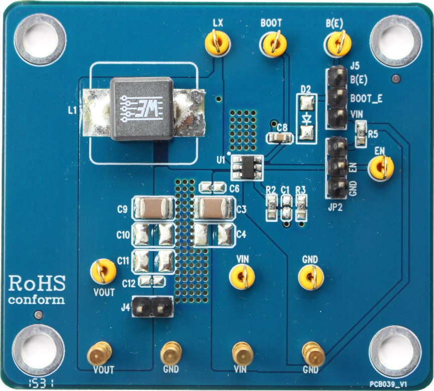
Please carefully inspect the EVB IC and external components, comparing them to the following Bill of Materials, to ensure that all components are installed and undamaged. If any components are missing or damaged during transportation, please contact the distributor or send e-mail to evb_service@richtek.com
Test Points
The EVB is provided with the test points and pin names listed in the table below.
|
Test point/
Pin name
|
Signal
|
Comment (expected waveforms or voltage levels on test points)
|
|
VIN
|
Input voltage
|
Power input.
|
|
EN
|
Enable test point
|
Floating this pin or connecting this pin to GND can disable the device and connecting this pin to logic high can enable the device.
|
|
GND
|
Ground
|
System Ground. Provides the ground return path for the control circuitry and low-side power MOSFET.
|
|
BOOT
|
Bootstrap supply test point
|
Bootstrap Supply for High-Side Gate Driver. Connect a 0.1µF or greater capacitor from LX to BOOT to power the high-side switch.
|
|
FB
|
Feedback Voltage Input.
|
This pin is used to set the desired output voltage via an external resistive divider. The feedback voltage is 0.8V typically.
|
|
LX
|
Switch node test point
|
LX is the switching node that supplies power to the output and
connect the output LC filter from LX to the output load.
|
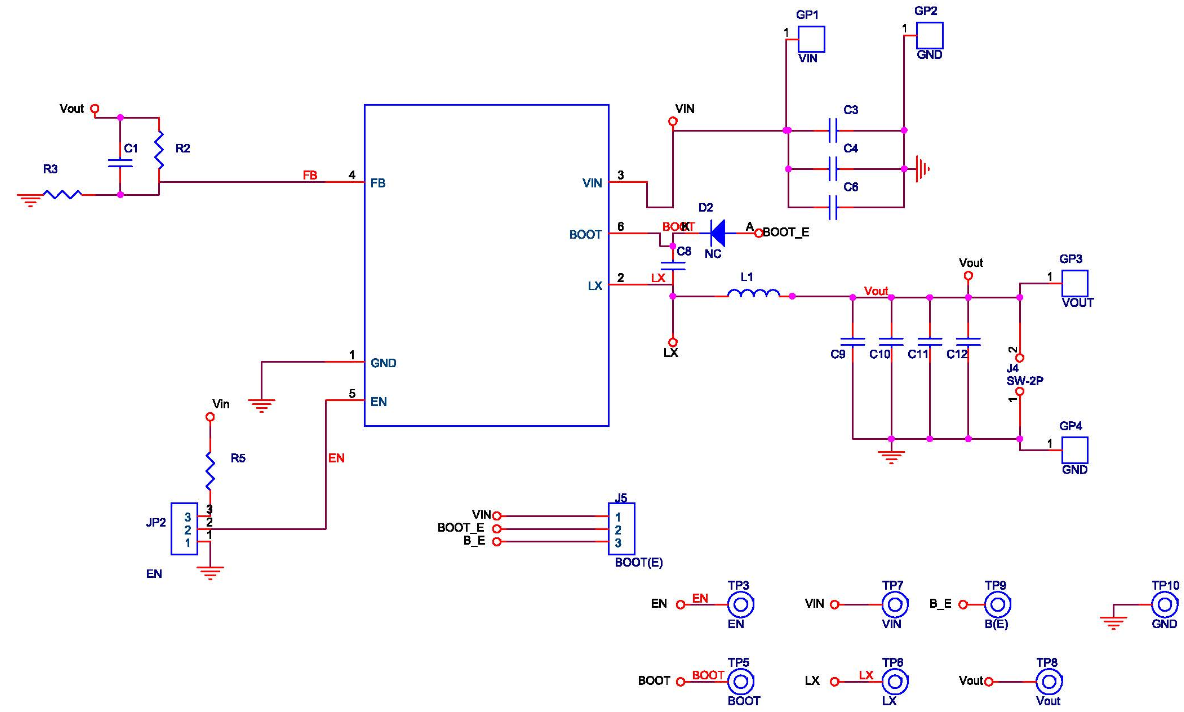
Power-up & Measurement Procedure
1. Apply a 12V nominal input power supply (4.5V < VIN < 18V) to the VIN and GND terminals.
2. Set the jumper at JP2 to connect terminals 2 and 3, connecting EN to enable operation.
3. Verify the output voltage (approximately 1.2V) between VOUT and GND.
4. Connect an external load up to 2A to the VOUT and GND terminals and verify the output voltage and current.
Output Voltage Setting
Set the output voltage with the resistive divider (R2, R3) between VOUT and GND with the midpoint connected to FB. The output is set by the following formula :

Schematic, Bill of Materials & Board Layout
EVB Schematic Diagram
Bill of Materials
|
Reference
|
Qty
|
Part Number
|
Description
|
Package
|
Manufacture
|
|
U1
|
1
|
RT6212AHGJ6F
|
DC/DC Converter
|
TSOT-23-6 (FC)
|
RICHTEK
|
|
C3, C9
|
2
|
C3225X5R1E226MT
|
22µF/25V/X7R
|
C-1210
|
TDK
|
|
C8
|
1
|
C1608X7R1H104K080AA
|
0.1µF/±10%/50V/X7R
|
C-0603
|
TDK
|
|
C1, C4, C6, C10, C11, C12, D2
|
7
|
|
N/A
|
|
|
|
R2
|
1
|
|
12kΩ
|
R-0603
|
|
|
R3
|
1
|
|
24kΩ
|
R-0603
|
|
|
R5
|
1
|
|
100kΩ
|
R-0603
|
|
|
L1
|
1
|
7443340220
|
2.2µH/12.5A
|
8.4 x 7.9 x 7.2 mm
|
WE
|
PCB Layout
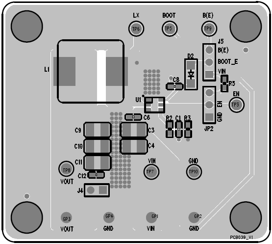
Top View (1st layer)
PCB Layout—Inner Side (2nd Layer)
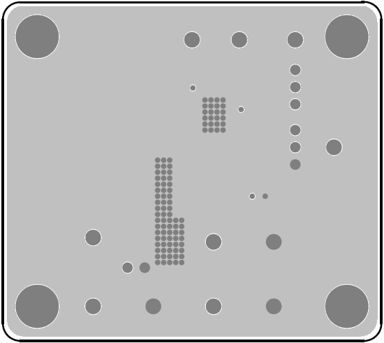
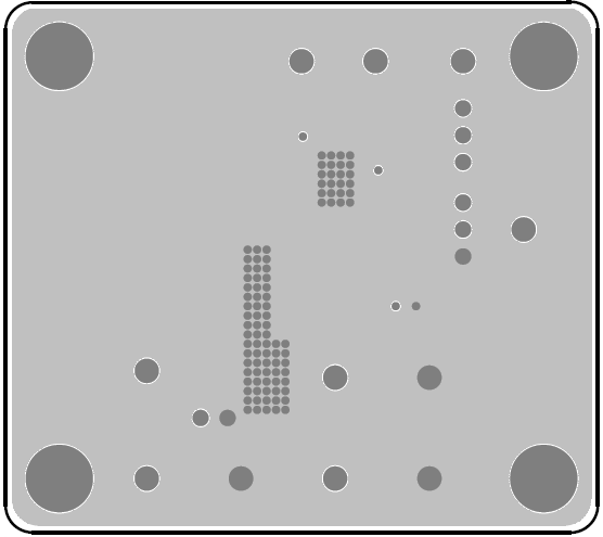
PCB Layout—Inner Side (3rd Layer)
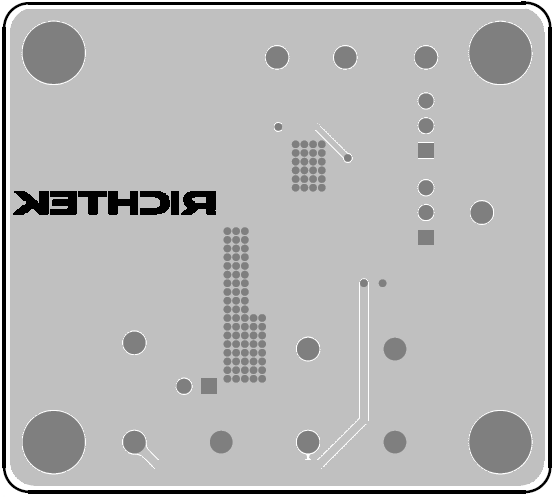
Bottom View (4th Layer)